

Home
 Our Products By Equipment Refurbished Equipment
Refurbished Equipment
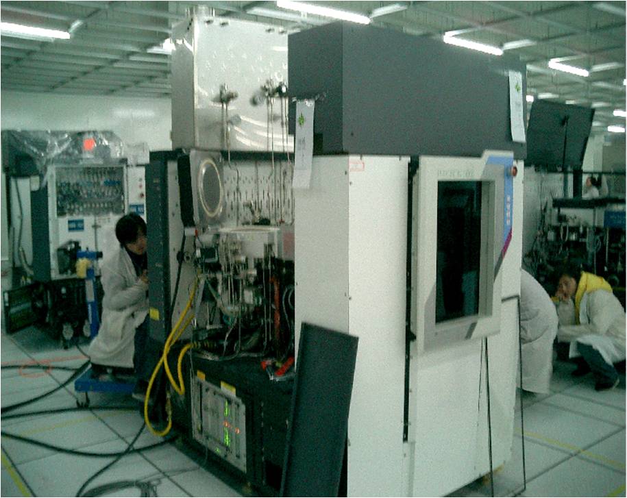


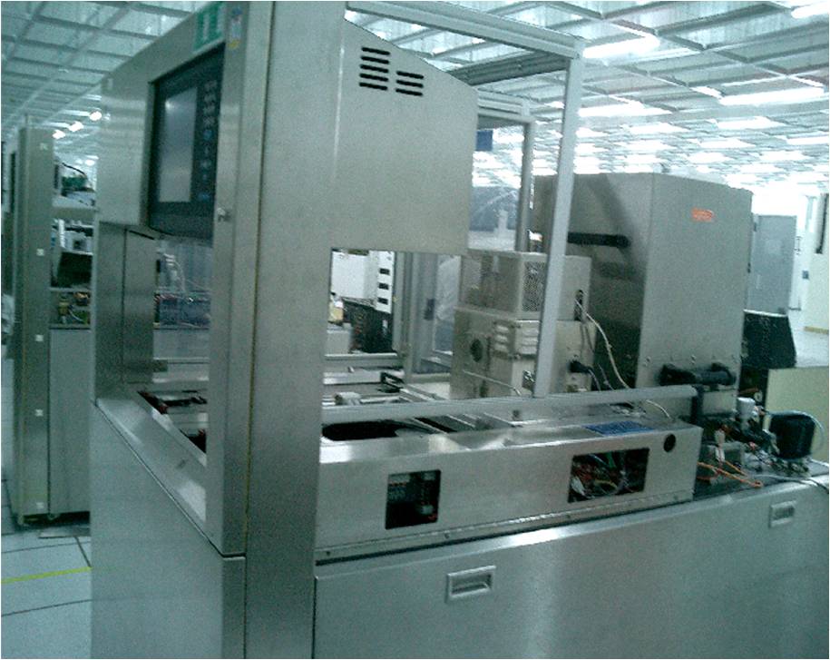
AP / PECVD Systems
- Oxide -
- Nitride -
- Tungsten -
- Tungsten Silicide -
- TEOS -
- PSG -
- Nitride -
- Tungsten -
- Tungsten Silicide -
- TEOS -
- PSG -
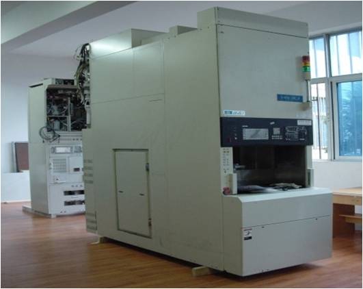
APCVD Systems
- Reduce Wafer Surface Contamination -
- Increase Repeatability of Manufacturing-Process Results -
- Increase Repeatability of Manufacturing-Process Results -
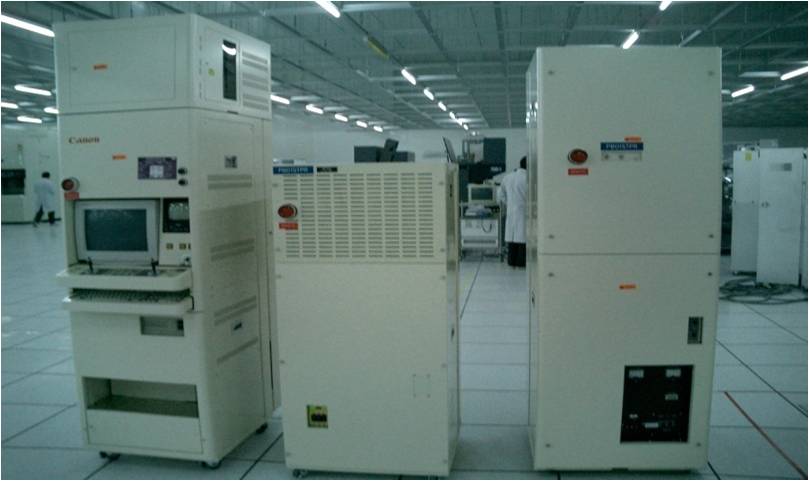
Aligner, Stepper and Scanner
- Contact Mask Align & Expose -
- G-line, i-line and DUV stepper -
- DUV Scanner -
- G-line, i-line and DUV stepper -
- DUV Scanner -
Coating, Developing, Cleaning Track
- SOG coating -
- Photo Resist Coating -
- Photo Resist Developing -
- Photo Resist Stripping -
- Wafer Cleaning -
- Photo Resist Coating -
- Photo Resist Developing -
- Photo Resist Stripping -
- Wafer Cleaning -
Hitachi CD SEM
- Computer-Controlled Stage Drive & Speed -
- Dual Cassette Loading -
- Auto-load to Loader Chamber -
- Arm Type Robot -
- Schottky Emission Type Electron Gun -
- Dual Cassette Loading -
- Auto-load to Loader Chamber -
- Arm Type Robot -
- Schottky Emission Type Electron Gun -
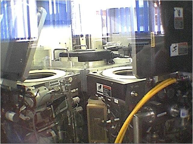
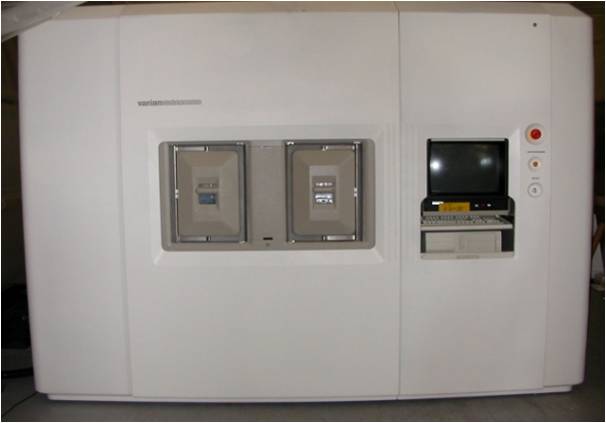
ION Implantation System
- High Current Implantation -
- Medium Current Implantation -
- High Energy Implantation -
- Medium Current Implantation -
- High Energy Implantation -
LAM Plasma Etcher
- PE / RIE / TCP Etching -
- PE / RIE / TCP, Oxide / Nitride / Metal Applications -
- Auto / Manual operation -
- PE / RIE / TCP, Oxide / Nitride / Metal Applications -
- Auto / Manual operation -
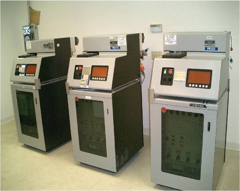
Oxidation Diffusion Furnace
- Diffusion -
- Annealing -
- Oxide -
- Nitride -
- TEOS -
- BPSG -
- Annealing -
- Oxide -
- Nitride -
- TEOS -
- BPSG -
Plasma Asher
- Bulk Resist Stripping -
- Implant Resist Stripping -
- Remove Scum -
- Isotropic Etching -
- Coating oxide / nitride etching -
- Surface Cleaning -
- Implant Resist Stripping -
- Remove Scum -
- Isotropic Etching -
- Coating oxide / nitride etching -
- Surface Cleaning -
Rapid Thermal Processor
- RTA-Ion implantation annealing -
- RTO-thin oxide -
- RTN nitride -
- Silicidation – titanium silicide -
- Titanium nitride -
- RTO-thin oxide -
- RTN nitride -
- Silicidation – titanium silicide -
- Titanium nitride -
For more infomation: Contact Us